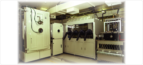
We are conducting several application research projects, such as, the usage of Photo-excited CVD developed by "Miyazaki Oki Electric Co., Ltd." as a leveling membrane in the thin film encapsulation of organic EL. Photo-excited CVD is considered to be the best technique for embedded films.

Thin film deposition by the CVD (Chemical Vapor Deposition ) method is a very important step in the manufacturing process of semiconductor devices and FPDs. At present, the thin films are deposited mainly by thermal CVD, plasma CVD and atmospheric pressure CVD. However, the next-generation semiconductor devices and organic EL require a low-damage process using neither high temperature of over 400-C nor plasma.
The photo-chemical vapor deposition method (VUV-CVD method) using vacuum ultraviolet light uses only photon energy to deposit a film by efficiently decomposing a material gas. The VUV-CVD of low temperature and low damage is optimum for flat film in the over coating deposition step of the organic EL manufacturing process.

As shown in Fig. 1, the bond energy of the material TEOS is 8.3eV for Si-O, 3.7eV for C-O, 3.6eV for C-C and 4.3eV for C-H. As opposed to it, the photon energy of a xenon excimer lamp is very high energy of 7.2eV. Therefore, it is possible to cut the bonds other than Si-O and deposit an oxide film on a substrate.

Fig. 2 shows the growth rate for various meterial grases. The growth rate of the VUV-CVD method significantly depends on the material gas. The gas C is capable of high-speed film deposition of over 300nm/min.

Fig.3 shows an example of applying a VUV-CVD film to a semiconductor device. By using the VUV-CVD film as an interlayer film between wirings, a flat film with good gap filling can be deposited without using CMP (Chemical Mechanical Polishing).